93
9140CINDCO02/10
ATA8741
generation. Similarly, do not write the TCNT0 value equal to BOTTOM when the counter is
down-counting.
The setup of the OC0x should be performed before setting the Data Direction Register for the
port pin to output. The easiest way of setting the OC0x value is to use the Force Output Com-
pare (0x) strobe bits in Normal mode. The OC0x Registers keep their values even when
changing between Waveform Generation modes.
Be aware that the COM0x1:0 bits are not double buffered together with the compare value.
Changing the COM0x1:0 bits will take effect immediately.
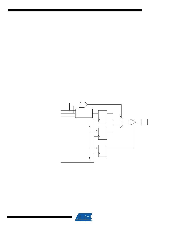
20.6 Compare Match Output Unit
The Compare Output mode (COM0x1:0) bits have two functions. The Waveform Generator uses
the COM0x1:0 bits for defining the Output Compare (OC0x) state at the next Compare Match.
Also, the COM0x1:0 bits control the OC0x pin output source. Figure 20-4 on page 93 shows a
simplified schematic of the logic affected by the COM0x1:0 bit setting. The I/O Registers, I/O
bits, and I/O pins in the figure are shown in bold. Only the parts of the general I/O Port Control
Registers (DDR and PORT) that are affected by the COM0x1:0 bits are shown. When referring
to the OC0x state, the reference is for the internal OC0x Register, not the OC0x pin. If a system
reset occur, the OC0x Register is reset to
0
.
Figure 20-4. Compare Match Output Unit, Schematic
The general I/O port function is overridden by the Output Compare (OC0x) from the Waveform
Generator if either of the COM0x1:0 bits are set. However, the OC0x pin direction (input or out-
put) is still controlled by the Data Direction Register (DDR) for the port pin. The Data Direction
Register bit for the OC0x pin (DDR_OC0x) must be set as output before the OC0x value is visi-
ble on the pin. The port override function is independent of the Waveform Generation mode.
The design of the Output Compare pin logic allows initialization of the OC0x state before the out-
put is enabled. Note that some COM0x1:0 bit settings are reserved for certain modes of
operation, see
Register Description
on page 100
PORT
DDR
D Q
D Q
OCn
Pin
OCnx
D Q
Waveform
Generator
OMnx1
OMnx0
0
1
OCn
lk
发布紧急采购,3分钟左右您将得到回复。
相关PDF资料
ATA8742-PXQW
MCU W/TRANSMITTER ASK/FSK 24QFN
ATA8743-PXQW
MCU W/TRANSMITTER ASK/FSK 24QFN
ATAVRRZ200
KIT DEMO AT86RF230
AV101-12LF
ATTENUATOR HIP3 0.70-1GHZ 8-SOIC
AV102-12LF
ATTENUATOR HIP3 1.7-2GHZ 8SOIC
AV113-12LF
ATTENUATOR HIP3 2.1-2.3GHZ 8SOIC
AXUV100G
SENSOR ELECTRON DETECTION
B0205F50200AHF
XFRMR BALUN RF 200-500MHZ 1608
相关代理商/技术参数
ATA8742
制造商:ATMEL 制造商全称:ATMEL Corporation 功能描述:Microcontroller with UHF ASK/FSK Transmitter
ATA8742C- PXQW
制造商:Atmel Corporation 功能描述:Embedded C incl RF Tx for 433 MHz
ATA8742C-PXQW
功能描述:8位微控制器 -MCU RoHS:否 制造商:Silicon Labs 核心:8051 处理器系列:C8051F39x 数据总线宽度:8 bit 最大时钟频率:50 MHz 程序存储器大小:16 KB 数据 RAM 大小:1 KB 片上 ADC:Yes 工作电源电压:1.8 V to 3.6 V 工作温度范围:- 40 C to + 105 C 封装 / 箱体:QFN-20 安装风格:SMD/SMT
ATA8742C-PXQW-1
功能描述:EMBEDDED INCL RF TX FOR 433 MHZ 制造商:microchip technology 系列:- 包装:剪切带(CT) 零件状态:在售 频率:429MHz ~ 439MHz 应用:通用 调制或协议:UHF 数据速率(最大值):32kbps 功率 - 输出:7.5dBm 电流 - 传输:9.8mA 数据接口:SPI 天线连接器:PCB,表面贴装 存储容量:4kB 闪存,256B EEPROM,256B SRAM 特性:- 电压 - 电源:2 V ~ 4 V 工作温度:-40°C ~ 85°C 封装/外壳:24-VQFN 裸露焊盘 标准包装:1
ATA8742-PXQW
功能描述:8位微控制器 -MCU Embedded uC incl RF Tx for 433 MHz
RoHS:否 制造商:Silicon Labs 核心:8051 处理器系列:C8051F39x 数据总线宽度:8 bit 最大时钟频率:50 MHz 程序存储器大小:16 KB 数据 RAM 大小:1 KB 片上 ADC:Yes 工作电源电压:1.8 V to 3.6 V 工作温度范围:- 40 C to + 105 C 封装 / 箱体:QFN-20 安装风格:SMD/SMT
ATA8743
制造商:ATMEL 制造商全称:ATMEL Corporation 功能描述:Microcontroller with UHF ASK/FSK Transmitter
ATA8743C- PXQW
功能描述:8位微控制器 -MCU Embedded uC incl RF Tx for 315 MHz
RoHS:否 制造商:Silicon Labs 核心:8051 处理器系列:C8051F39x 数据总线宽度:8 bit 最大时钟频率:50 MHz 程序存储器大小:16 KB 数据 RAM 大小:1 KB 片上 ADC:Yes 工作电源电压:1.8 V to 3.6 V 工作温度范围:- 40 C to + 105 C 封装 / 箱体:QFN-20 安装风格:SMD/SMT
ATA8743C-PXQW
制造商:Atmel Corporation 功能描述:EMBEDDED ?C INCL RF TX FOR 868 MHZ - Trays 制造商:Atmel Corporation 功能描述:EMBEDDED C INCL 868MHZ TX